Xilinx Kintex Ultrascale+ FPGA Pattern Generator
This FPGA pattern generator project involved the development of a bespoke high-speed electronics and firmware platform for a quantum computing application. The system combines a Xilinx Kintex Ultrascale+ FPGA with programmable high-speed I/O, picosecond timing control, external communications and an FMC mezzanine interface for laboratory testing and commissioning.
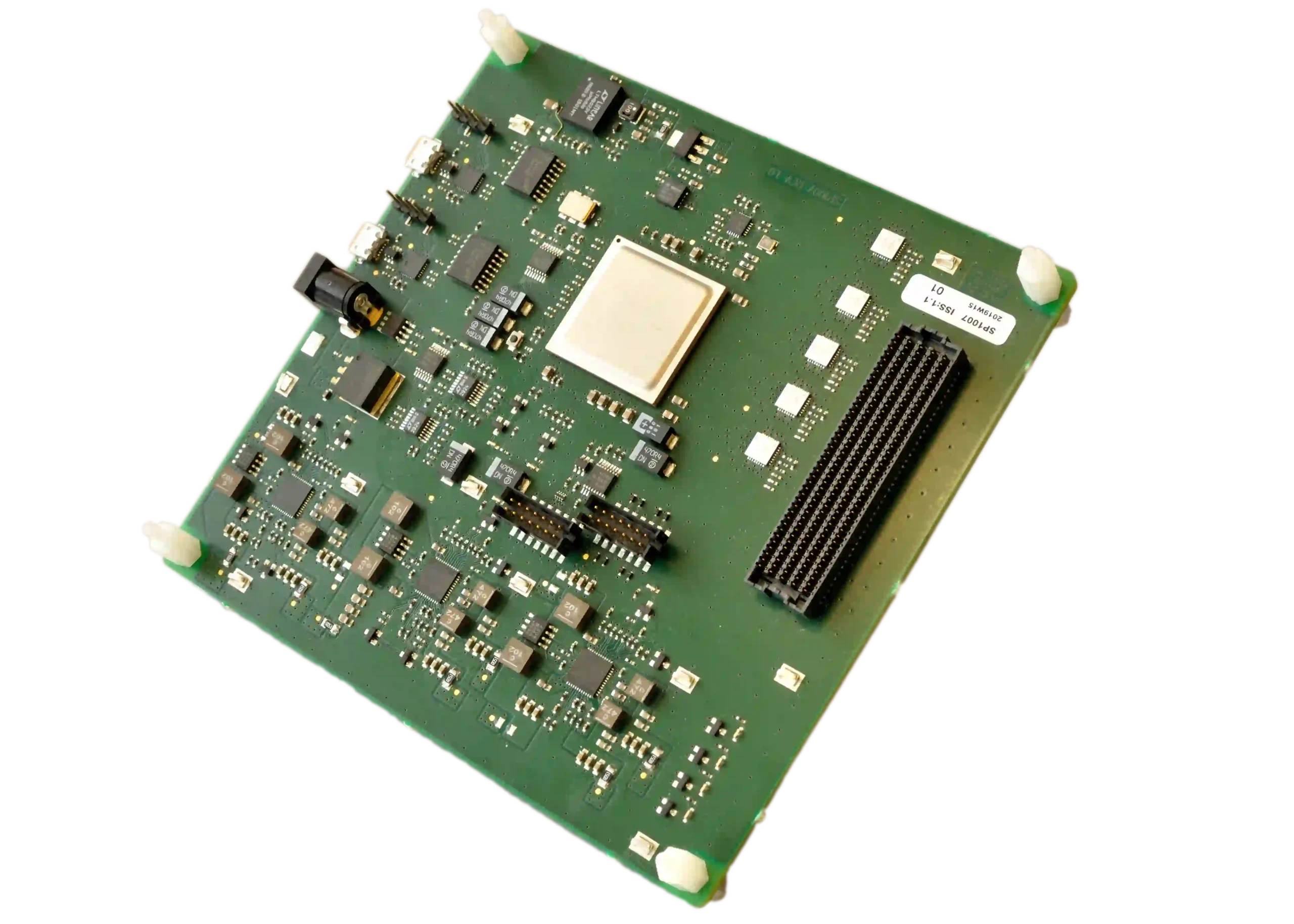
FPGA Pattern Generator Key Features:
- Xilinx Kintex Ultrascale+ FPGA: XCKU5P device with 6.25GHz I/O lines.
- MicroBlaze Control: FPGA-based MicroBlaze processor for system control.
- Picosecond Timing: Analog Devices HMC856 wideband 28Gbps digital time-delay ICs with 3ps resolution.
- Programmable Patterns: USB and UART interfaces allow customisation and user-programmable patterns.
- FMC Mezzanine: High-speed I/O exposed through an FMC connector for system testing and commissioning.
- Signal Integrity: Simulated and laboratory-tested differential routing and termination networks.
- Power Sequencing: Carefully designed supplies and sequencing for the FPGA’s multiple voltage rails.
- High-Speed Firmware: Custom FPGA firmware generates customer-specific digital patterns and interfaces.
FPGA Pattern Generator System Architecture:
The centre of the system is the Xilinx Kintex Ultrascale+ FPGA with an embedded MicroBlaze processor. Around the FPGA are external interfaces including JTAG, USB, RS232 and FMC mezzanine connectivity, together with memory, clocks, timing circuits, digital delay devices and the customer’s proprietary silicon.
The design also includes the required power supplies and sequencing circuitry for the FPGA voltage rails, enabling the hardware and firmware development to progress as an integrated platform.

Xilinx Kintex Ultrascale+ FPGA PCB:
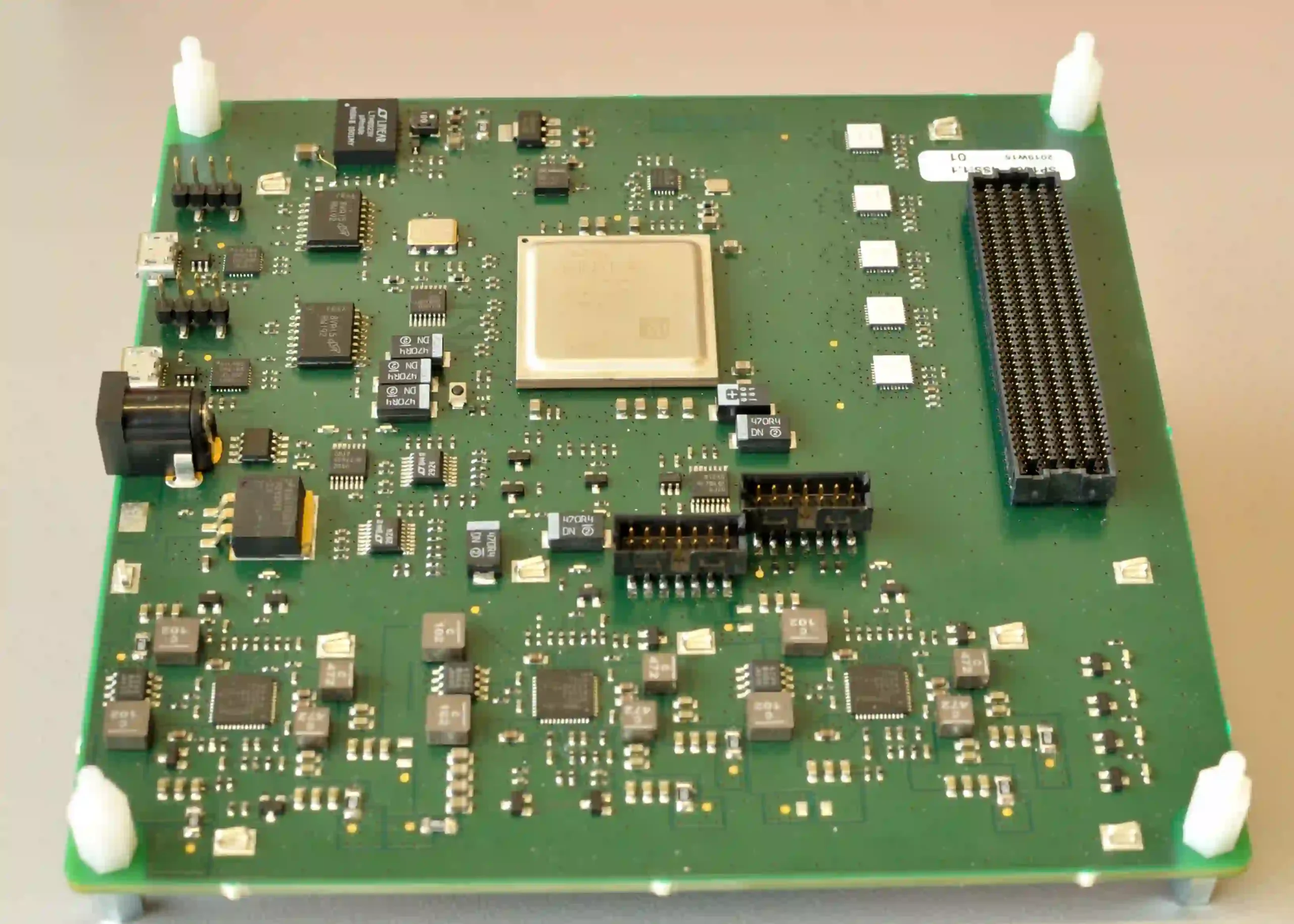
The custom PCB is built around the Kintex Ultrascale+ FPGA and carries the major processing, timing and interface components required by the application.
Alongside the FPGA are the FMC mezzanine connector, wideband digital time-delay devices, system clocks, external communications and supporting power circuitry.
16-Layer High-Speed PCB Design:
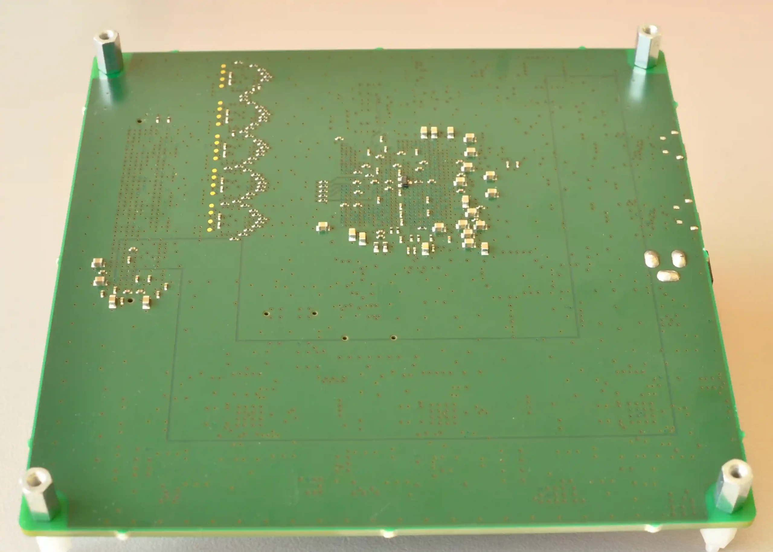
The PCB uses a 16-layer stack-up with multiple signal layers and power planes to support the high-speed digital architecture.
Impedance-matched differential routing and carefully selected termination networks were designed, simulated and laboratory tested to maintain signal integrity across the customer-specific high-speed interfaces.
FMC Mezzanine & Test Connectivity:
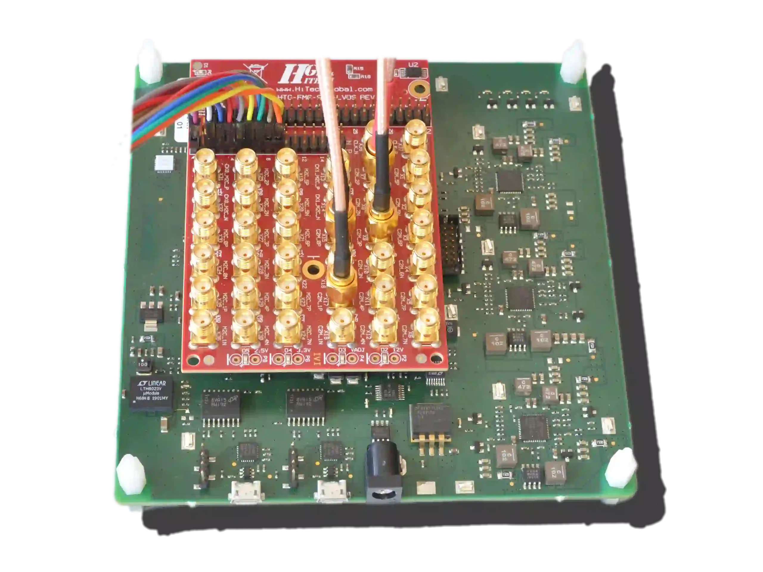
The FMC mezzanine interface exposes the system’s high-speed I/O to external test equipment, supporting development, system integration and commissioning.
Using an off-the-shelf mezzanine alongside the custom FPGA PCB helped provide flexible laboratory connectivity while reducing the amount of application-specific hardware required.
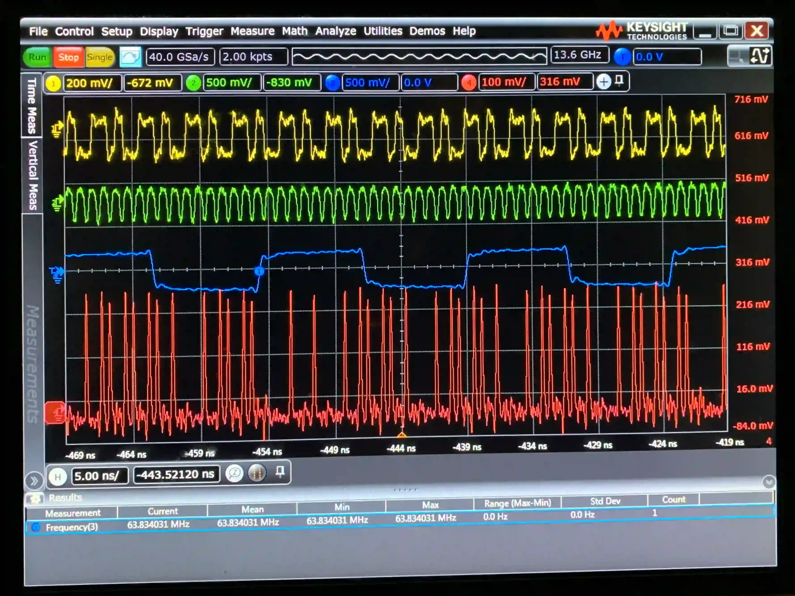
Picosecond Timing & High-Speed Validation:
The platform uses Analog Devices HMC856 wideband digital time-delay ICs with 3ps timing resolution and supports customer-specific high-speed I/O generated by the combined hardware and FPGA firmware.
The original case study records 160ps signals during validation, with the high-speed differential interfaces verified through simulation, prototyping and laboratory testing.
FPGA Firmware & Turnkey Development:
The firmware stores the required pattern data in RAM and uses the custom high-speed interface to generate the customer’s digital signals. USB and UART connectivity allow patterns to be customised and controlled externally.
Spark completed the electronics design, FPGA firmware, prototyping, testing and technical demonstrations as a turnkey development programme. The completed system was signed off by the customer, with Spark continuing to support additional electronics and firmware projects.